
About CoolCAD
CoolCAD is located in the Washington, DC, metropolitan area, and has strong relationships with government, industry and academic institutions in the area. We have direct access to various government laboratories and agencies allowing us collaborate with key decision makers interested in SiC technology. We also have close connections with the University of Maryland (UMD) in College Park, and leverage talent and resources present at this flagship research institute.
Our CoolCAD Team possess a unique combination of expertise in electronics, excelling in semiconductor physics, fabrication, design, and integrated and board-level circuit development and manufacturing. Together we have published over 100 research papers in professional scientific and engineering journals and have multiple patents on our key discoveries in the area of wide bandgap SiC electronics.

CoolCAD is a leader in the development and fabrication of SiC-based power devices and high-temperature electronics for many industries including aerospace, automotive, defense, geothermal development, green energy generation, industrial furnace control, water purification and oil and gas extraction.
As of Today, CoolCAD has been awarded 21 Phase I SBIRs (Small Business Innovation Research grants), 8 Phase II SBIRs, and several beyond-Phase II awards matched by investors and contracts. Additionally, CoolCAD has been chosen for many service and R&D contracts, awarded by other private companies.
In 2021, CoolCAD was awarded a multi-year contract from DARPA (Defense Advanced Research Projects Agency) for the development of high-temperature electronics.
In 2019, CoolCAD was awarded a patent for their silicon carbide integrated circuit active photodetector (Patent No. US 10,446,592 B1).
In 2017, CoolCAD was awarded a Phase II Small Business Innovative Research contract from National Aeronautics and Space Administration (NASA). They won the $750,000 award for their cutting-edge work in silicon carbide-based (SiC) wide bandgap electronics.
In 2010, CoolCAD began designing and fabricating their own SiC based electronic chips, becoming a member of a small group of elite companies in the World with this unique capability. It is this capability that led NASA to contract with CoolCAD to find solutions to high-temperature challenges for electronics used in space missions such as the exploration of Venus, imaging stars that not only emit visible light, but ultraviolet light as well, and for monitoring the Earth’s environment, especially the delicate ozone layer.
Founded in 2008 by University of Maryland ECE Professor Dr. Neil Goldsman and ECE graduate Dr. Akin Akturk, CoolCAD Electronics LLC started as a spinoff of UMD’s Electronics Modeling & Mixed Signal Group. The company began as a computer aided design (CAD) house supporting the development of electronic circuits for use at cryogenic temperatures in outer space and in the new field of quantum computing.
Founders

Dr. Neil Goldsman, Professor in the Department of Electrical and Computer Engineering (ECE) at the University of Maryland (UMD) at College Park, and Director of the Mixed Signal VLSI Design Laboratory, Distributed Sensor and Communication Networks Group, and the Semiconductor Simulation Laboratory, is an inventor and entrepreneur. His recent work focuses on ad-hoc sensor networks, high temperature and cryogenic electronics, and semiconductor device modeling. His research has attracted over four million dollars of support for the University of Maryland and his work has been sponsored by leading governmental and industrial organizations including NSF, SRC, NSA, ARL, ONR, ARO, DHS, NIH and Intel Corporation. Dr. Goldsman has supervised the design of over 50 integrated circuits (ICs), received multiple awards for his research and has published more than one hundred fifty peer-reviewed technical papers. Most recently, Dr. Goldsman has focused on commercializing his research, whereupon he received 7 patents. Dr. Goldsman received his Ph.D. from Cornell University with a minor in Applied Physics and major in Electrical Engineering.
Dr. Akin Akturk earned his M.S and Ph.D. degrees from the University of Maryland, College Park. He is the recipient of the NASA Tech Brief Award for his design of a hybrid AlGaN-SiC photodiode for deep UV photon detection. His recent work includes performance and thermal modeling of nanoscale MOSFETs and planar and three-dimensional integrated circuits. He has extensive non-isothermal modeling experience for devices such as SOI-MOSFETs and MOSFETs with silicon or heterojunctions in their channels. His analyses cover a wide temperature spectrum, from cryogenic temperatures to hundreds of degrees above room temperature. Through simulation, he demonstrated the concept of using thermal conduits to remove heat from chips and along with his colleagues was awarded a patent for chip heat removal by the US patent office. Dr. Akturk has designed and fabricated several ICs for temperature sensing and has published multiple technical papers on full-chip heating and novel MOSFET configurations.

Facility
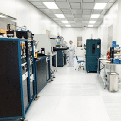
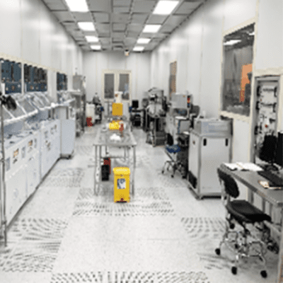
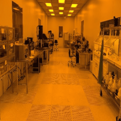
Our facility is state-of-the-art, underscoring our commitment to meet the highest quality standards, and is equipped for scientific research, computer modeling, new product development, environmental testing and prototyping of SiC electronic devices. Our proprietary chip design and prototype fabrication processes utilize equipment for high-temperature oxidation, photolithography, dry plasma etching and metal deposition.
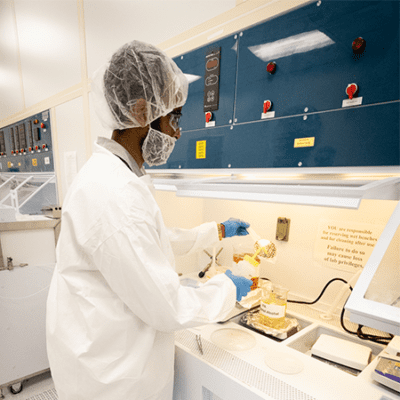
Wet bench processing of SiC wafer in NANOFAB
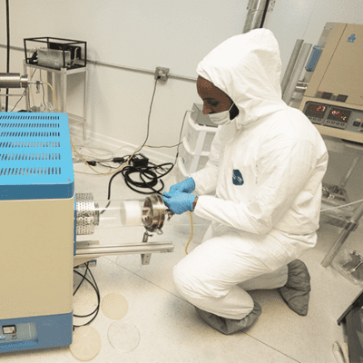
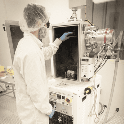
Loading SiC wafers into oxidation furnace
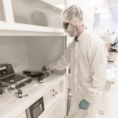
Photoresist spinning process
Exposure of photoresist in micron-scale mask alignment process
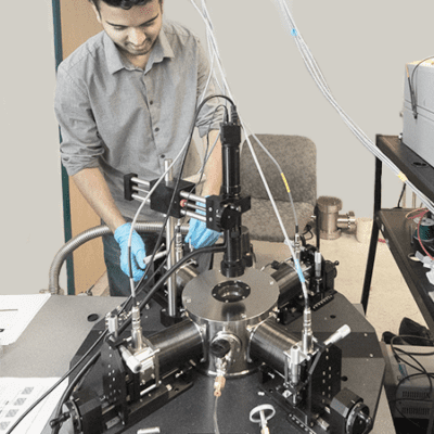
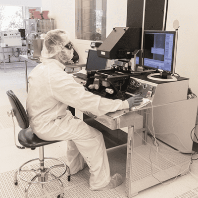
Probe station for cryogenic testing
Electron beam evaporator for metal layer deposition
Metal deposition tunnel
Etching tunnel
Photolithography tunnel